Kawasaki & Daihen’s Impact on Wafer Handling Robotics
Published: 2025-09-11
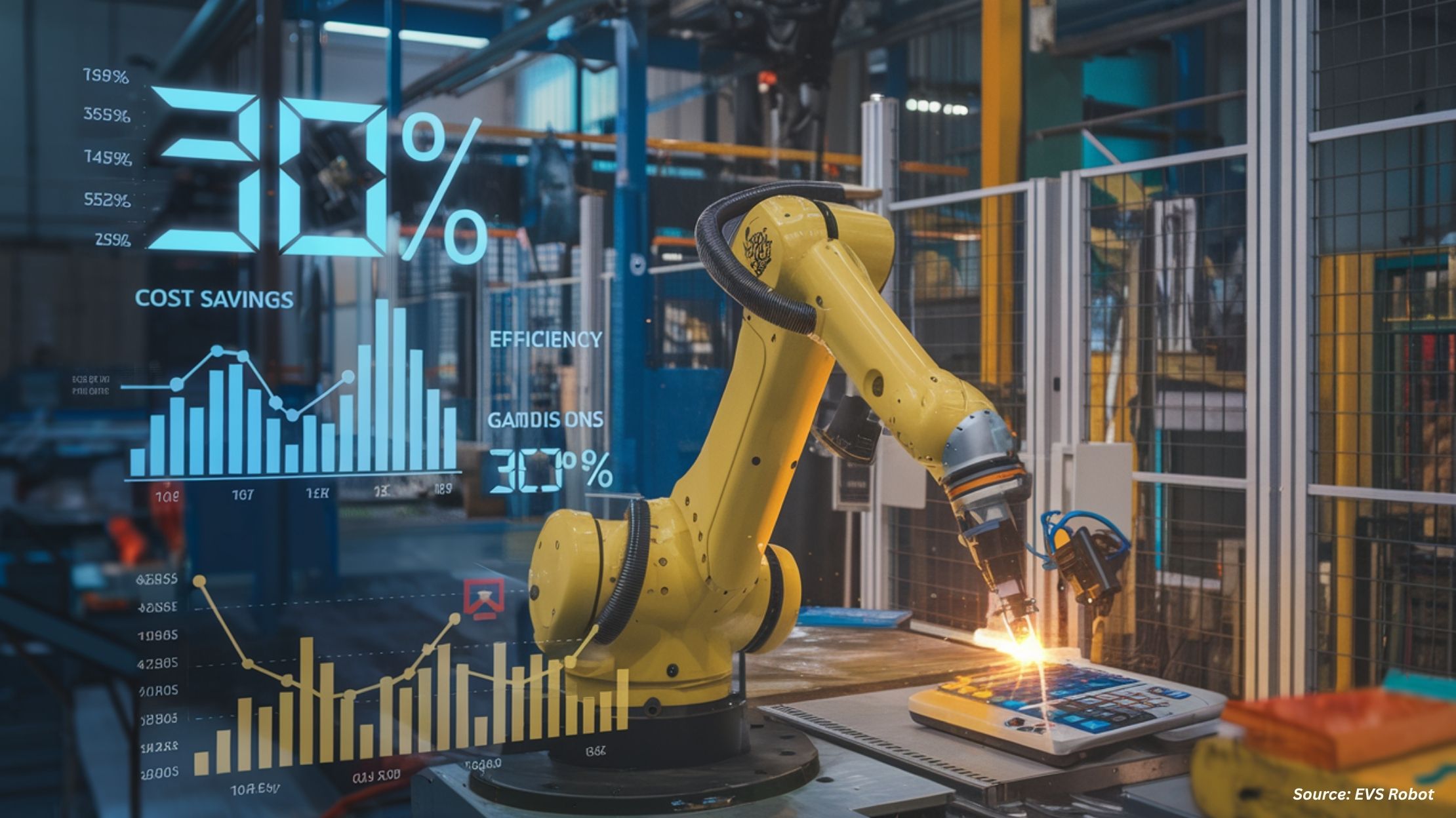
The Wafer Handling Robots Market, estimated at USD 1.60 billion in 2023, is anticipated to rise to USD 3.37 billion by 2030, experiencing 1x growth with a CAGR of 10.5% from 2024-2030. This surge in market value is propelled by increasing automation requirements and technological advancements in AI and machine learning. These innovations are enhancing the performance and efficiency of wafer handling robots, addressing the growing demand for sophisticated semiconductor manufacturing solutions.
Wafer Handling Robots Market Overview
The wafer handling robots market is experiencing rapid growth, fueled by advancements in semiconductor manufacturing and automation technologies. As the demand for high-performance electronics and microchips increases, there is a rising need for precise and efficient wafer handling solutions. These robots help in ensuring the safe transfer and positioning of wafers during various stages of semiconductor production, thereby minimizing contamination risks and enhancing production efficiency. Key technologies driving this market include robotic arms with advanced sensors and AI-based control systems, enabling high precision and speed in handling delicate wafers. Additionally, the integration of these robots with smart manufacturing systems and IoT devices is enabling real-time monitoring and optimization of production processes, further boosting operational efficiency.
The wafer handling robots market is set for substantial growth, powered by breakthroughs in robotics, AI, and IoT technologies. Emerging opportunities include the development of sophisticated robots capable of handling increasingly smaller and thinner wafers, as well as solutions tailored for specific semiconductor manufacturing environments. These advancements open up new avenues for companies to lead in the highly competitive semiconductor industry.
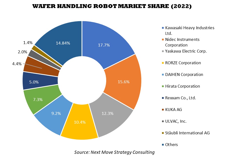
In this dynamic market, several key players are making substantial contributions through innovation and technological expertise. Companies such as Kawasaki Heavy Industries Ltd., Yaskawa Electric Corp., Daihen Corporation, Hirata Corporation, and ULVAC, Inc. are at the forefront, driving the industry's evolution. Their cutting-edge products and solutions are setting new benchmarks for precision, reliability, and efficiency in wafer handling, shaping the future of semiconductor manufacturing.
For the latest market share analysis and in-depth wafer handling robots industry insights: Download FREE Sample
Highlights of Kawasaki Heavy Industries Ltd.
Kawasaki Heavy Industries Ltd. is the leading company in the precision machinery and robotics sector, with a strong focus on the development of wafer handling robots. These robots are critical in the semiconductor manufacturing process, where precision and reliability are essential to ensuring the quality and efficiency of production. Kawasaki’s extensive experience in robotics enabled the company to create cutting-edge solutions that meet the stringent demands of wafer handling, providing accurate and consistent movement of delicate wafers throughout various stages of manufacturing.
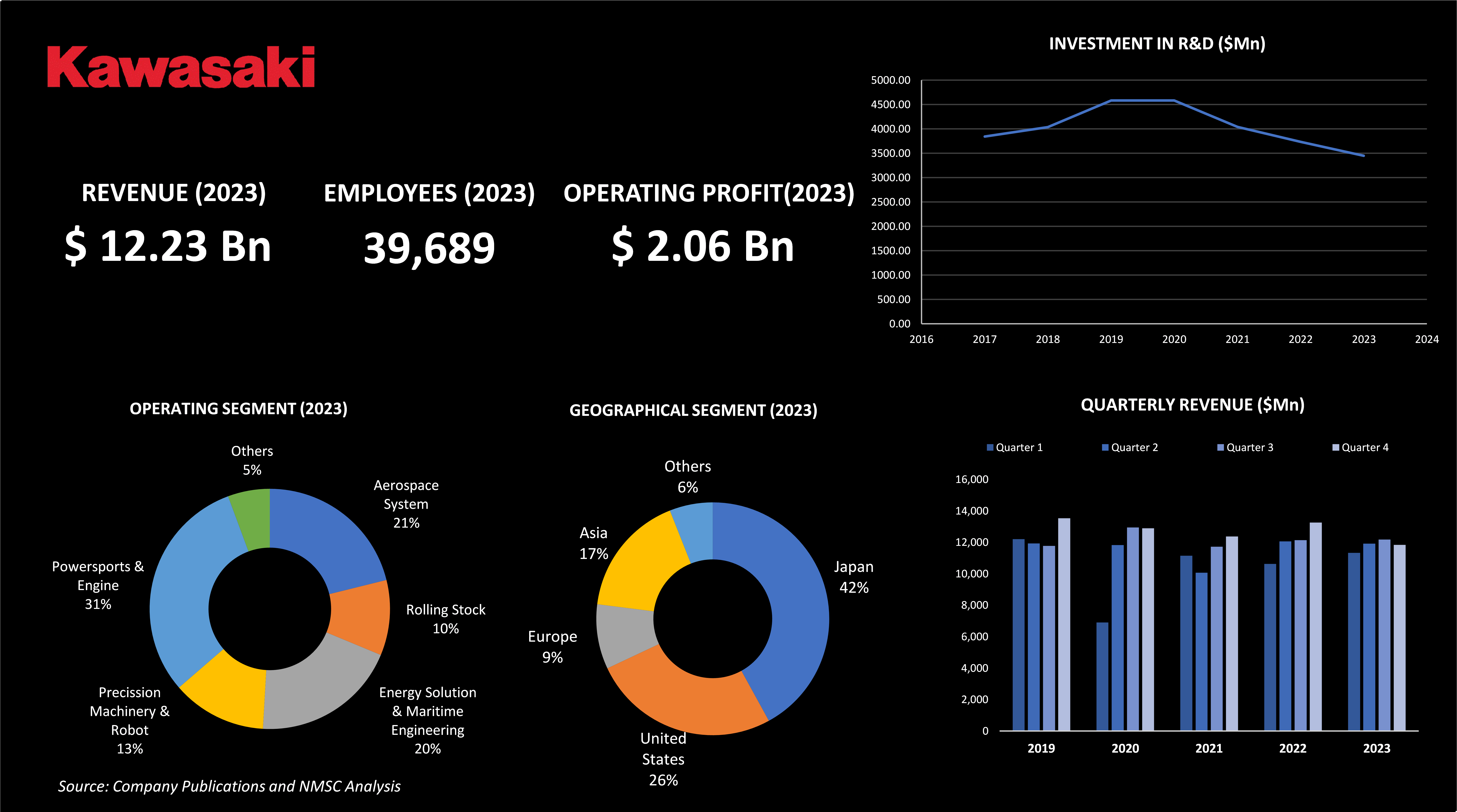
In 2023, Kawasaki Heavy Industries reported revenues of USD 12.23 billion, alongside an operating profit of USD 2.06 billion. The company’s operations include several key segments, including aerospace systems, rolling stock, energy solutions and maritime engineering, precision machinery and robotics, and powersport and engine. Kawasaki's global reach is reflected in its revenue distribution, with 42% of its income generated in Japan, 26% in the USA, 9% in Europe, and 17% in Asia, highlighting its strong international presence. The company is currently investing heavily in future growth as part of its Group Vision 2030, recognizing the need for substantial upfront investments to secure long-term success. This strategy is pivotal in maintaining the company’s competitive edge and driving technological innovation across its various business segments, including robotics.
Kawasaki Heavy Industries Ltd. continues to strengthen its position in the wafer handling market by investing in advanced research and development initiatives. A key initiative in Kawasaki’s innovation efforts is the establishment of “Future Lab HANEDA” on April 2022. Located at Haneda Innovation City, this facility is dedicated to the open-innovation-based development of robotics products and services. It serves as a hub for demonstrating and testing new robotic technologies in real-life scenarios, furthering Kawasaki’s commitment to pioneering advancements in the field.
These advancements are vital for the semiconductor industry, where the slightest deviation result in costly production issues. Kawasaki’s robots are engineered to minimize such risks, ensuring that wafers are handled with the highest level of care and accuracy, thereby contributing to the overall efficiency and quality of semiconductor manufacturing processes. Through its relentless pursuit of innovation and strategic investments, Kawasaki Heavy Industries is positioned to lead the market in wafer handling robotics. The company’s dedication to advancing these technologies is in line with its broader vision of driving growth and maintaining its position as one of the global leaders in precision machinery and robotics.
Highlights of Yaskawa Electric Corporation
Yaskawa Electric Corporation is making significant advancements in the wafer handling robot market, leveraging its extensive expertise in motion control and robotics to deliver innovative solutions that meet the stringent demands of the semiconductor industry. The company is recognized for its advanced robotics technology, that ensures precision, speed, and reliability in the delicate process of handling semiconductor wafers.
In 2024, Yaskawa Electric Corporation reported revenues of USD 3834.5 million reflecting a 3.5% increase compared to the previous year. The company's operating profit for the same period was USD 441.1 million, a decrease of 3.0%, while profit before tax stood at USD 460.52 million, down by 2.9%. Despite these slight decreases, Yaskawa maintained a strong overall financial performance, with total comprehensive income reaching USD 70,452 million, a 2.6% decrease.
Furthermore, Yaskawa's operations are organized into three key segments, motion control, robotics, and system engineering that forms the backbone of the company’s business, driving the development of its wafer handling robots. The extensive presence of the company at global level is evident in its regional revenue breakdown, with 34% of earnings coming from Japan, 21% from Americas, 17% from Europe, and 28% from Chinas. This widespread geographical distribution allows Yaskawa to effectively cater to varied markets and reinforces its standing as a leader in the global robotics sector.
Recognizing the rising demand for electric vehicles (EVs), with their increasing reliance on semiconductors for everything from power management to autonomous driving systems, Yaskawa launched the Motoman Next series, an industry-first adaptive robot platform designed to tackle social issues through advanced automation. This innovative platform enhances flexibility and efficiency in automotive manufacturing, particularly for EVs, by integrating advanced adaptive capabilities and automation solution. This initiative positioned Yaskawa at the forefront of the next wave of industrial robotics.
Moreover, Yaskawa also focus on increasing automation and labor-saving measures at its production bases in Japan and overseas. These efforts are aimed at building an efficient and resilient production system that can quickly adapt to changes in market demand. This approach is essential for maintaining the high standards required in the semiconductor industry, where Yaskawa’s wafer handling robots are critical for ensuring the smooth and precise handling of wafers. The company’s commitment to innovation is further demonstrated by its increased investments in research and development. In 2022, Yaskawa’s R&D expenses rose by USD 4.14 million, reflecting the dedication of the company in enhancing the reliability and efficiency of its wafer handling robots.
Yaskawa Electric Corporation continues to advance the technology behind wafer handling robots, ensuring that its solutions meet the evolving needs of the semiconductor industry. By integrating AI and IoT technologies, Yaskawa is positioning itself to meet future industry demands, including carbon-neutral initiatives and the growing market for port cranes in Asia. Additionally, by making strategic investments and concentrating on its core business areas, Yaskawa continues to be a prominent player in wafer handling robotics market while also advancing semiconductor manufacturing.
Highlights of Daihen Corporation
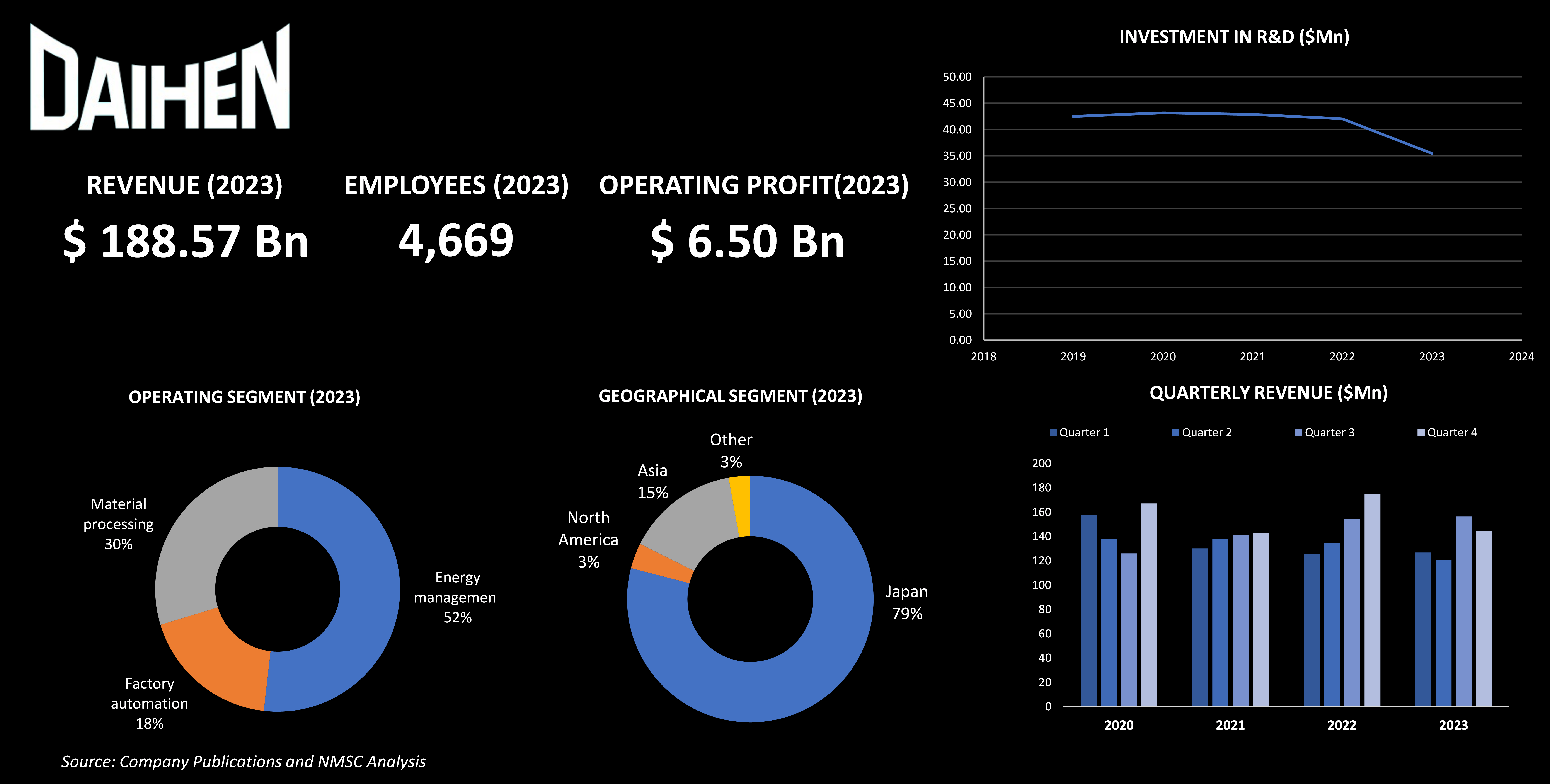
Daihen Corporation stands as one of the major players in the wafer handling robot market, known for its substantial impact and strategic advancements. With a robust revenue stream of USD 188 billion and a dedicated workforce of 4,669 employees in 2023, the company operates across multiple global regions, including Japan, North America, Asia, and other areas.
The strategic initiatives of the company are vital in driving growth within the wafer handling sector. The company's recent acquisition of the German system integrator Femitech in May 2022 highlights its commitment to enhancing system integration capabilities and expanding its range of robot-related products. This move is part of the company’s broader strategy to provide comprehensive solutions that cater to the evolving needs of customers around the world.
In addition, Daihen Corporation's increasing R&D expenditures, with investments of USD 51 million in 2020, USD 49 million in 2021, and slightly varying figures in subsequent years, reflect its strong commitment to innovation. This sustained investment is closely linked to advancements in the wafer handling robot market. By continuously enhancing its research and development efforts, Daihen is driving technological progress and reinforcing its leadership position in the industry, ensuring that its wafer handling solutions remain at the forefront of automation and semiconductor manufacturing.
Highlights of Hirata Corporation
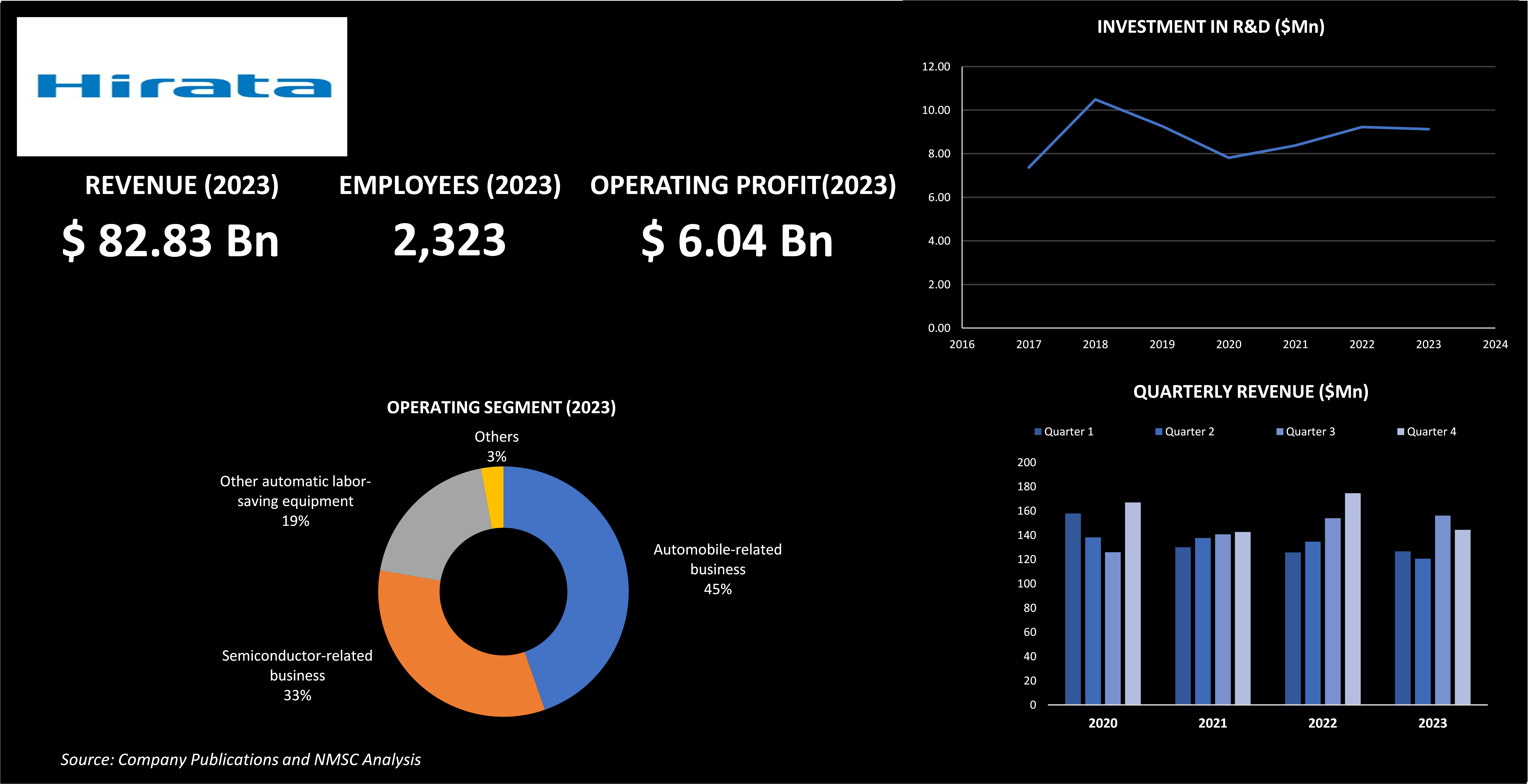
Hirata Corporation, one of the key players in the wafer handling robot market, has shown impressive performance in the fiscal year, 2024. Despite navigating a challenging economic environment characterized by geopolitical tensions, rising costs, and fluctuating exchange rates, Hirata has demonstrated resilience and growth. For the fiscal year 2024, Hirata reported net sales of approximately USD 82.83 billion, reflecting a 5.6% increase year on year. The company achieved an operating profit of about USD 6.04 billion, up 2.2% from the previous year. Additionally, ordinary profit rose by 7.9% to approximately USD 0.043 billion.
Hirata capitalized on strong demand for its silicon wafer transfer equipment in the wafer handling robot market, driven by substantial orders from manufacturers in the electric vehicle (EV) sector. The growth of the sector contributed to an improved cost of sales ratio for semiconductor-related equipment. Specifically, Hirata's semiconductor-related business achieved firm net sales of around USD189.2 million, despite a 5.4% decline from the previous year. Operating profit in this segment surged by 29.2% to about USD 30.7 million, highlighting the company's effective cost management and strong market position.
In contrast, other segments faced challenges. The automobile-related business saw increased EV-related capital investment, with net sales reaching approximately USD 255.5 million, up 22.1% year on year. Operating profit for this segment also grew by 5.9% to about USD11.4 million. However, the automatic labor-saving equipment segment, which includes organic electroluminescence (organic EL) and home appliances, experienced declines, with net sales falling to around USD 110.2 million and operating profit decreasing by 87.1% to approximately USD 0.8 million.
Moreover, the advancements of the company in wafer handling robots highlights its commitment to innovation and efficiency. The company remains at the forefront of developing high-performance equipment crucial for semiconductor manufacturing, including state-of-the-art silicon wafer transfer solutions. Leveraging its expertise in automation and precision engineering, the company is well-positioned to address the evolving demands of the wafer handling robot market and maintain its competitive edge.
Highlights of Ulvac Inc.
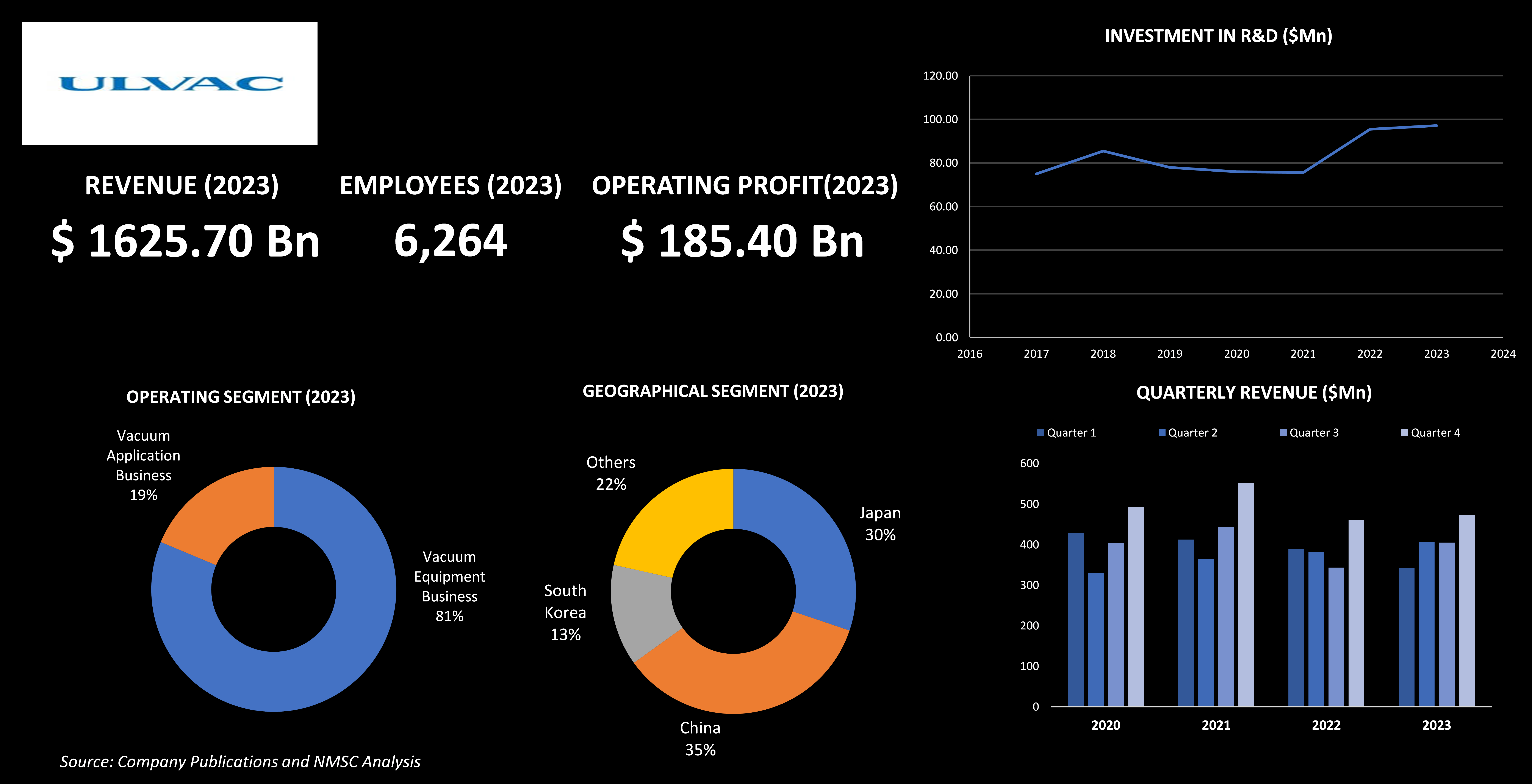
ULVAC, Inc., headquartered in Chigasaki, Kanagawa, Japan, is one of the leading players in the development and production of advanced vacuum equipment and technologies, including wafer handling robots. Established in 1952, the company has a strong presence across key markets, notably Japan, China, South Korea, and other regions. The operations of the company are divided into two main segments, the vacuum equipment business, which accounts for 81% of its total revenue, and the vacuum application business, contributing 19%. In the recent fiscal year, ULVAC reported a significant increase in net sales, reaching USD 1625.70 billion. The company’s operating profit rose by 49.3% to USD 185.40 billion, reflecting robust market performance.
As the future business environment evolves, ULVAC is currently experiencing a surge in demand for its wafer handling robots, driven by medium- to long-term investment expansion in semiconductor-related areas such as logic and memory. The growing need for semiconductors, fueled by advancements in digitalization, generative AI, big data, and IoT, is directly impacting ULVAC's wafer handling robots by increasing the demand for precision and efficiency in handling complex semiconductor wafers. Additionally, the establishment of local supply chains by central governments is already leading to the adoption of ULVAC's cutting-edge wafer handling technologies to meet this rising semiconductor demand. In the electronics field, present investments in power devices, the shift to green energy, and the rise of electric vehicles (EVs) are further driving the need for ULVAC's sophisticated wafer handling robots. This demand is evident as ULVAC's robots are increasingly being utilized in the mass production of EV batteries, where they ensure precise and safe handling, contributing to advancements in battery size, capacity, and safety. These ongoing developments are positioning ULVAC's wafer handling robots as essential tools in today's evolving semiconductor and electronics industries, reinforcing the company's commitment to innovation and technological leadership.
ULVAC remains committed to innovation, with research and development (R&D) investments totaling USD 15.60 billion, a notable increase from the previous year. This R&D expenditure represents 6.1% of net sales, highlighting the company's focus on future growth and technological advancement. A key initiative in this regard is the establishment of the ULVAC Advanced Technology Collaborative Research Cluster in partnership with Tokyo Institute of Technology, aimed at fostering cutting-edge research in vacuum technology and related fields. In the field of wafer handling robots, ULVAC is actively pursuing development initiatives to enhance the precision, efficiency, and integration capabilities of its robots, aligning with the semiconductor industry's evolving needs. These efforts reflect the commitment of the company in maintaining its leadership position in the market and contributing to the advancement of semiconductor manufacturing technology.
Have questions? Inquire before purchasing the full report: https://www.nextmsc.com/wafer-handling-robots-market/inquire-before-buying
Summary of Wafer Handling Robots Market
The Wafer Handling Robots market is currently driven by the increasing adoption of automation and advanced technologies, with companies prioritizing efficiency and cost reduction. As the demand for precision and speed in semiconductor manufacturing grows, industries are investing in wafer handling robots to streamline operations and minimize labour costs. The integration of AI and machine learning is enhancing these robots' capabilities, leading to improved accuracy and performance. This trend is expected to continue, with further advancements in automation likely to propel market growth. Companies are increasingly relying on these technologies to stay competitive and meet the evolving demands of the semiconductor industry.
About the Author
 Sukanya Dey is a passionate and insightful writer with over three years of experience, she excels in providing clients with in-depth research and valuable insights, helping them navigate complex business challenges. She has a keen interest in various industries, including Healthcare, Manufacturing, Automotive, Robotics, and ICT & Media. Sukanya strives to offer fresh perspectives and innovative solutions through her comprehensive research. She finds immense joy in weaving her thoughts and ideas into captivating articles and blogs, where her passion for literature and art shines through. In her free time, she enjoys reading books, cooking, filming, often drawing inspiration from these activities for her creative writing endeavours.
About the Reviewer
 Debashree Dey is a skilled Content Writer, PR Specialist, and Assistant Manager with strong expertise in Digital Marketing. She specializes in crafting visibility strategies and delivering impactful, data-driven campaigns. Passionate about creating engaging, audience-focused content, she helps brands strengthen their online presence. Beyond work, she draws inspiration from creative projects and design pursuits.





Add Comment