Wafer Probe Market by Type (Manual, Semi-automatic, and Fully Automatic), and by Application (Integrated Device Manufacturer (IDMs), Outsourced Semiconductor Assembly and Test (OSAT), Research Institute, and Others) – Global Opportunity Analysis and Industry Forecast 2024-2030
Wafer Probe Market Overview
The global Wafer Probe Market size was valued at USD 2.43 billion in 2023 and is predicted to reach USD 3.77 billion by 2030 with a CAGR of 6.5% from 2024-2030.
The wafer probe market also known as semiconductor probe, encompasses the development of specialized testing equipment used in the semiconductor industry. This equipment is essential for examining and validating the performance of integrated circuits (ICs) and chips directly on a semiconductor wafer during the fabrication process. This market plays a vital role in maintaining the functionality and reliability of semiconductors by providing essential solutions such as electrical probes, contact probes, and advanced testing technologies to meet the growing requirements of modern electronics, ensuring the seamless performance of semiconductor components across various industries.
Market Dynamics and Trends
The growing adoption of electronics such as smartphones, laptop and wearable devices drives the demand for semiconductor probe, as more advanced and miniaturized electronic devices require precise testing and quality control to meet performance standards.
According to UN Trade & Development (UNCTAD) the smartphones shipment reached 1.2 billion in 2023. The substantial growth in electronic device production highlights the heightened need for reliable testing solutions, propelling the market growth.
Moreover, the rising adoption of electric vehicles (EVs), coupled with technological advancements such as advanced driver assistance systems (ADAS) and infotainment systems, drives the demand for sophisticated semiconductor chips. This increased need for high-performance chips leads to a higher demand for wafer probes to ensure these components meet rigorous quality and performance standards.
As per the report published by the International Energy Agency, the adoption of electric vehicles (EVs) is increasing at a significant rate, with sales of electric cars rising to approximately 14 million in 2023, up from 10.5 million in 2022. The surge in adoption of EVs drives the demand for efficient charging systems that enhance the charging experience, thereby fueling the growth of the market. The expansion in automotive industry drives the demand for reliable wafer probing, fuelling of the wafer probe market growth.
Furthermore, the rising semiconductor manufacturing is driving the growth of the wafer probe industry, as the production of semiconductor devices increases, there is a greater need for quality control and testing to ensure each chip meets performance standards. This growing manufacturing activity drives demand for wafer probes, that are essential for verifying the reliability and functionality of semiconductor components.
As per the latest report published by the Semiconductor Industry Association (SIA), the global semiconductor sales reached USD 149.9 billion in the second quarter of 2024, representing an increase of 18.3% as compared to second quarter of 2023. The surge in sale of semiconductor drives the demand for efficient testing solutions.
However, the high cost of advanced testing equipment hinders the growth of the market particularly for the smaller semiconductor manufacturers and research institutions.
On the contrary, the integration of 3D technology into semiconductor probe stations is expected to create ample opportunities in the coming years. The integration of 3D technology into wafer probe stations will allow for more precise and accurate testing of semiconductor devices improving the performance and efficiency of the testing process.
For instance, in June 2024, Samsung plans to introduce a 3D HBM (High-Bandwidth Memory) chip packaging service. This service will allow Samsung to package HBM chips in a 3D configuration, that will enable much smaller chip sizes compared to traditional packaging methods.
Market Segmentations and Scope of the Study
The wafer probe market report is segmented on the basis of type, application and region. On the basis of type, the market is divided into manual, semi-automatic, and fully automatic. On the basis of application, the market is classified into integrated device manufacturer (IDMs), outsourced semiconductor assembly and test (OSAT), research institute, and others. Regional breakdown and analysis of each of the aforesaid segments include regions comprising of North America, Europe, Asia-Pacific, and RoW.
Geographical Analysis
Asia-Pacific holds the dominant in wafer probe market share and is expected to continue its dominance during the forecast period. The rising demand for consumer electronics that utilize advanced semiconductors in this region is driving the wafer probe industry, as the need for precise testing of these semiconductors increases to ensure their performance and reliability. According to the Shanghai Municipal People's Government, retail sales in China's consumer electronics market are anticipated to increase by 4 percent, reaching USD 305 billion in 2023. The growth rate is expected to accelerate to 5 percent in 2024. This expansion highlights the crucial role of wafer probes in supporting the semiconductor industry's evolving testing needs.
Moreover, the expanding semiconductor market in countries such as India, China, and South Korea is further driving the growth of the market. As semiconductor production increases in the Asia-Pacific countries, there is a heightened need for wafer probe stations to test and ensure the quality of the growing volume of chips. According to the India Brand Equity Foundation, the semiconductor market in India is undergoing notable growth with reaching a value of USD 26.3 billion in 2022, and it is projected to reach USD 271.9 billion by 2032. This growth emphasizes the growing wafer probe market demand for advanced testing solutions, positioning wafer probe stations as a crucial component in supporting the semiconductor industry's development.
On the other hand, North America is expected to show a steady rise in the wafer probe market. The growing adoption of electric vehicles (EVs) in this region is driving the wafer probe sector because the increased demand for advanced semiconductors in EVs requires more precise testing to ensure their quality and performance. According to the latest report published by the International Council on Clean Transportation, the sale of electric light-duty vehicles reached about 1.4 million, up from nearly 1 million in 2022. This significant growth in EV adoption is increasing demand for high-quality semiconductor testing, thereby driving continued expansion in the wafer test equipment market in the region.
Moreover, in North America, the expansion of data centers and the growing demand for high-performance computing are driving the wafer test equipment market, as these factors increase the need for semiconductors that require precise testing. According to projections by McKinsey & Company, demand for data centers in the U.S. is projected to increase by approximately 10% annually through 2030. Such rise in the data centers increases the need for advanced testing solutions to meet the operational efficiency of the semiconductors used in the data centers.
Competitive Landscape
Various key players operating in the wafer probe industry include FormFactor, Inc., ERS electronic GmbH, MPI Corporation, D-Coax, TOKYO SEIMITSU CO., LTD, MICRONICS JAPAN CO.,LTD., Wentworth Laboratories, Semiprobe, Hprobe GmbH, The Micromanipulator Company, SEMISHARE CO., LTD., TSE Co., Ltd., Tokyo Electron Limited, Complete Probe Solutions Inc., SPEA S.p.A., and others. These companies are adopting various strategies such as product launches to remain dominant in the wafer test equipment market.
For instance, in December 2022, Hitachi Ltd. launched a wafer surface inspection system with high throughput and sensitivity named LS9600.The new inspection system featured a new system for detecting particles and defects on non-patterned wafer surfaces in semiconductors along with reducing inspection costs.
Moreover, in July 2022, Rohde & Schwarz GmbH & Co KG launched a wafer device characterization test solution for the full radiofrequency performance of semiconductors. The new wafer device provides semiconductor manufacturers to perform reliable and repeatable on-wafer device testing in the development, product qualification, and in production phase.
Furthermore, in May 2022, ERS electronic GmbH launched a temperature calibration device ProbeSense. The new device uses the XYZ axis motion capability of the prober and the sensor measures the temperature over several points on the wafer surface.
Key Benefits
-
The wafer probe market report provides the quantitative analysis of the current market and estimations from 2024 to 2030. This analysis assists in identifying the prevailing market opportunities to capitalize on.
-
The study comprises of a detailed analysis of the current and future wafer probe market trends for depicting the prevalent investment pockets in the industry.
-
The information related to key drivers, restraints, and opportunities and their impact on the wafer probe market is provided in the report.
-
The competitive analysis of the market players along with their market share in the wafer probe market is mentioned.
-
The SWOT analysis and Porter’s Five Forces model are elaborated in the study.
-
The value chain analysis in the market study provides a clear picture of the stakeholders’ roles.
Wafer Probe Market Key Segments
By Type
-
Manual,
-
Semi-automatic
-
Fully Automatic
By Application
-
Integrated Device Manufacturer (IDMs)
-
Outsourced Semiconductor Assembly and Test (OSAT)
-
Research Institute
-
Others
By Region
-
North America
-
The U.S.
-
Canada
-
Mexico
-
-
Europe
-
The U.K.
-
Germany
-
France
-
Italy
-
Spain
-
Denmark
-
Netherlands
-
Finland
-
Sweden
-
Norway
-
Russia
-
Rest of Europe
-
-
Asia-Pacific
-
China
-
Japan
-
India
-
South Korea
-
Australia
-
Indonesia
-
Singapore
-
Taiwan
-
Thailand
-
Rest of Asia-Pacific
-
-
RoW
-
Latin America
-
Middle East
-
Africa
-
Key Players
-
FormFactor, Inc.
-
ERS electronic GmbH
-
MPI Corporation
-
D-Coax
-
TOKYO SEIMITSU CO., LTD
-
MICRONICS JAPAN CO.,LTD.
-
Wentworth Laboratories
-
Semiprobe
-
Hprobe GmbH
-
The Micromanipulator Company
-
SEMISHARE CO., LTD.
-
TSE Co., Ltd.
-
Tokyo Electron Limited
-
Complete Probe Solutions Inc.
-
SPEA S.p.A.
REPORT SCOPE AND SEGMENTATION
|
Parameters |
Details |
|
Market Size in 2023 |
USD 2.43 billion |
|
Revenue Forecast in 2030 |
USD 3.77 billion |
|
Growth Rate |
CAGR of 6.5% from 2024 to 2030 |
|
Analysis Period |
2023–2030 |
|
Base Year Considered |
2023 |
|
Forecast Period |
2024–2030 |
|
Market Size Estimation |
Billion (USD) |
|
Growth Factors |
|
|
Countries Covered |
28 |
|
Companies Profiled |
15 |
|
Market Share |
Available for 15 companies |
|
Customization Scope |
Free customization (equivalent up to 80 working hours of analysts) after purchase. Addition or alteration to country, regional, and segment scope. |
|
Pricing and Purchase Options |
Avail customized purchase options to meet your exact research needs. |
")


About the Author
 Sikha Haritwal is an assistant manager with strong expertise in market research, data analysis, and cross-functional coordination. She plays a key role in leading complex research initiatives, strengthening analytical rigor, and enabling data-driven decision-making across teams. Known for her leadership mindset and structured problem-solving approach, she supports process improvement, enhances operational efficiency, and contributes to building scalable frameworks that drive long-term strategic outcomes and organizational effectiveness.
About the Reviewer
 Supradip Baul is an accomplished business consultant and strategist with over a decade of rich experience in market intelligence, strategy, technology, and business transformation. His work has included rigorous qualitative and quantitative analysis across multiple industries, helping clients shape investment decisions and long-term roadmaps. Earlier in his career, he was associated with Gartner, where he contributed to industry-leading reports and market share analyses. He has worked with leading global companies and holds an MBA with a dual specialization in Marketing and Finance.
At Next Move Strategy Consulting, we understand that insightful market research is the cornerstone of successful business decisions. That's why we employ a robust and multifaceted approach, combining various methodologies to deliver the most accurate and actionable data for our clients.

Research Landscape
We navigate the world of research with two primary approaches:
Qualitative Approach
Our qualitative research methodologies involve immersive techniques such as in-depth interviews, focus groups, and observational studies. By engaging directly with individuals and stakeholders, we uncover valuable insights that quantitative data alone may overlook.

Quantitative Research
In tandem with qualitative methodologies, NMSC leverages the power of Quantitative Research to provide a robust foundation of numerical insights. Through systematic data collection and analysis, we quantify patterns, preferences, and market trends, offering a comprehensive view of the business landscape.
Our quantitative research approach employs diverse tools, including surveys, experiments, and statistical modelling. These methodologies enable us to gather data from a large and representative sample, ensuring the statistical significance of our findings. By employing structured questionnaires and standardized data collection methods, we guarantee the reliability and validity of the information we present to our clients.
Quantitative research is particularly effective in measuring the prevalence of trends, assessing market size, and gauging the impact of various factors on consumer behavior. The numerical precision attained through this approach equips our clients with actionable insights, facilitating data-driven decision-making and strategy formulation.


Our Specialized Toolbox for Industry-Specific Market Research
We deploy a specialized arsenal of techniques tailored to meet your unique requirements. Here's a glimpse into our comprehensive toolbox:

Information Procurement
The stage entails acquiring market data or relevant information through various sources and methodologies.


Market Research Approach
We utilize both top-down and bottom-up approaches in market research analysis to achieve a comprehensive understanding of the market dynamics, leveraging the broad perspective of industry trends and macroeconomic factors alongside detailed insights from specific segments and individual companies.

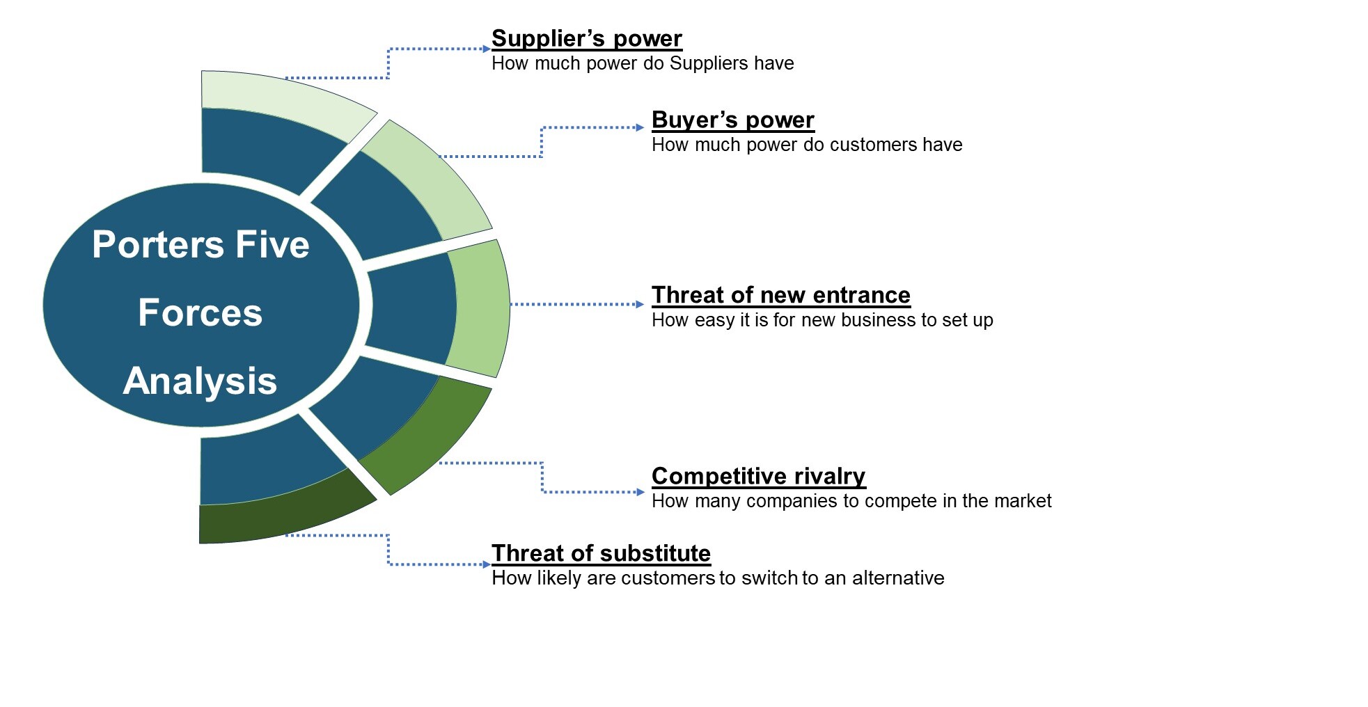
Porters Five Forces Analysis
We conduct Porter's Five Forces analysis to evaluate the competitive landscape of an industry, providing us with insights into factors that affect profitability and strategic positioning.
SWOT Analysis

Forecasting
We utilize a forecasting model to predict future consumption by considering parameters like population, economics, regulations, market competition, drivers, constraints, technology, and pricing. We also employ statistical techniques such as multilinear regression, exponential smoothing, moving average, ARIMA, and Monte Carlo simulations for accurate predictions. In econometric forecasting, we analyzed short-term and long-term event impacts, attributing values based on regulatory frameworks, economic factors, and market events.


 Speak to Our Analyst


 System Market")